EAGLE 7-es verzióig
1. Open the CAM proccessor
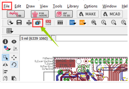
You can generate the Gerber file from the PCB editor. There are two ways to get to the editor. One of them is to click on the "CAM" button, (marked with red), the other is to go through "File -> CAM Processor".
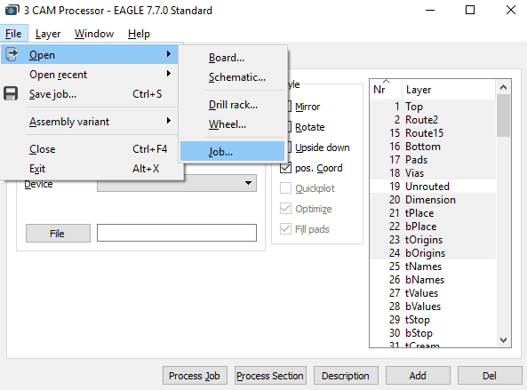
2. In the CAM Processor window select "File -> Open -> Job".
3. To generate the Gerber files select the correct CAM file for your software.
You can download the CAM files from down below:
4. Once downloaded the correct CAM file should be put into the EAGLE CAM folder. Navigate to the folder.
- If your PCB has a 2-layer design, choose "Nyakfutar_EAGLE_7.xx_2 layer.cam"
- If your PCB has a 4-layer design, choose "Nyakfutar_EAGLE_7.xx_4 layer.cam"
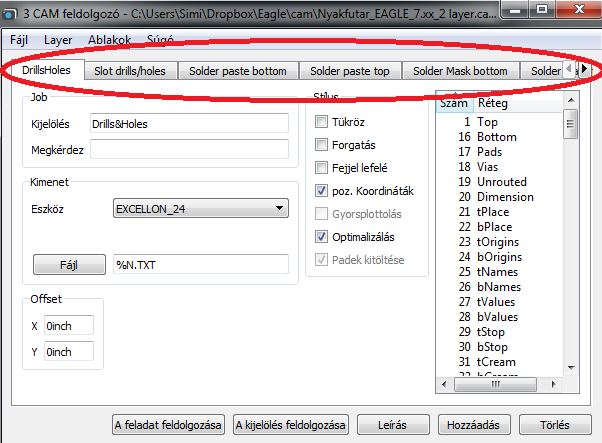
After selecting the file, click "Open". You can see the different layers as tabs on the top of the.
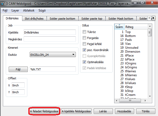
Press "Process Job" to generate the Gerber files. You will found these in the project folder.
EAGLE v.9
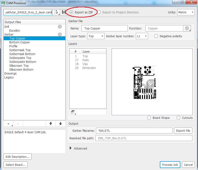
Exporting the Gerber files from EAGLE 9 is very similar to the previous version. The only difference is that you have to use a different CAM file, which you can download from here:
In the "CAM Processor" window choose the correct CAM file for your project then press the "Process Job" to generate the Gerber files.
When prompted give the location of the files.
You can check the "Export as ZIP" box (marked with red), which will pack the created files in a ZIP package immediately.
After generating the files, it is recommended you check them with a Gerber Viewer to see if everything is fine. Check the file extensions using the table below.
A Gerber állományok kiterjesztésének átírása
Extensions in case of 2 layers:
| Layer | Extension |
| Top Layer | pcbname.GTL |
| Bottom Layer | pcbname.GBL |
| Soldermask Top | pcbname.GTS |
| Soldermask Bottom | pcbname.GBS |
| Silk Top | pcbname.GTO |
| Silk Bottom | pcbname.GBO |
| NC Drill | pcbname.TXT / XLN |
| Mechanical Layer | pcbname.GKO / GML |
In case of one layer, only "Top" and "Bottom" files are required.
Additional Gerber files for 4 layers:
| Layer | Extension |
| Inner1 layer | pcbname.G2L / G1 |
| Inner2 layer | pcbname.G3L / G2 |
Increasing the number of layers on the PCB will result in a higher number of inner layers.


